Learn about IC CD4047 and the operating principle of the 4047 inverter circuit. Let’s discover the real-life applications of inverter circuits and how they impact our daily lives.
1. Power inverter
Power inverters are devices that can convert electrical energy of DC form into that of AC. They come in all shapes and sizes, from low power functions such as powering a car radio to that of backing up a building in case of power outage. Inverters can come in many different varieties, differing in price, power, efficiency and purpose. The purpose of a DC/AC power inverter is typically to take DC power supplied by a battery, such as a 12 volt car battery, and transform it into a 120 volt AC power source operating at 60 Hz, emulating the power available at an ordinary household electrical outlet.
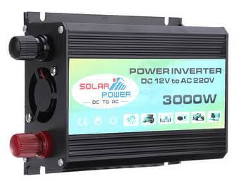
Power inverter DC 12V to AC 220V
Power inverters are used today for many tasks like powering appliances in a car such as cell phones, radios and televisions. They also come in handy for consumers who own camping vehicles, boats and at construction sites where an electric grid may not be as accessible to hook into. Inverters allow the user to provide AC power in areas where only batteries can be made available, allowing portability and freeing the user of long power cords.
On the market today are two different types of power inverters, modified sine wave and pure sine wave generators. These inverters differ in their outputs, providing varying levels of efficiency and distortion that can affect electronic devices in different ways. Usually sine wave inverters are more expensive then modified sine wave generators due to the added circuitry. This cost, however, is made up for in its ability to provide power to all AC electronic devices, allow inductive loads to run faster and quieter, and reduce the audible and electric noise in audio equipment, TV’s and fluorescent lights.
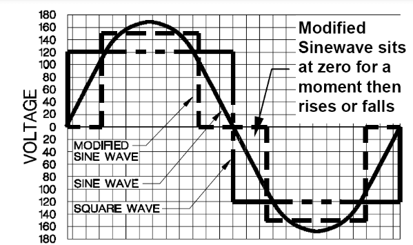
Square wave and sine wave
2. What is CD4047
The CD4047 is a high voltage multivibrator IC, that can operate in both Monostable and Astable mode. The IC requires an external resistor and capacitor to set the width of output pulse in monostable mode and the frequency of output pulse in Astable Mode. The monostable mode has positive and negative edge trigger with programmable pulse width. The Astable mode provides good frequency stability at 50% duty cycle.
The CD4047 IC can operate on 5V, 10V, 15V or even at 20V. The output of the IC always comes in TTL which makes it easy to work with other TTL devices and microcontrollers. The IC is commonly used in frequency discriminators, timing circuits, time-delay applications, envelope detection, frequency multiplication and division.
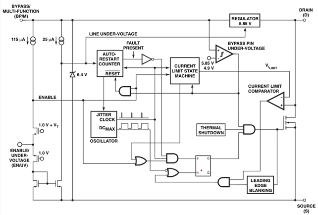
4047 logic block diagram
Features of CD4047 – Monostable/Astable Multivibrator IC
+ Wide Supply Voltage: 3.0V to 15V
+ High Noise Immunity
+ Buffered inputs
+ Requires only one external Resistor and Capacitor
+ Offers both monostable and astable mode operations
+ Low power consumption
+ Monostable Features: Duty-cycle approaches 100%, Retrigger option for pulse width expansion, positive/ negative edge trigger
+ Astable Features: 50% duty-cycle, Oscillator output available, good astable frequency stability
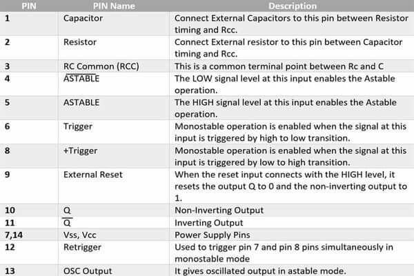
Functions of IC 4047 pins
3. CD4047 inverter circuit
The inverter circuit diagram that produces a square 220V voltage is drawn as shown below.
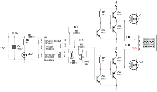
4047 inverter circuit
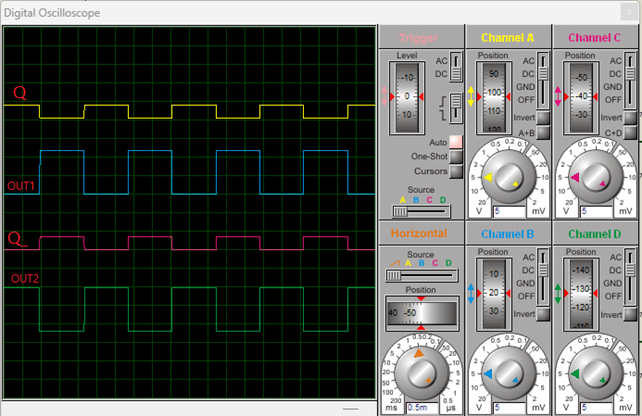
The circuit utilizes IC CD4047 to generate oscillating pulses. This IC produces two output pulses, Q and Q, with reverse phase, and these pulses can alter frequency. Frequency adjustment is achieved by modifying the capacitor value at pin 1 and the resistor value at pin 2. For simplicity, the circuit employs a 390k resistor in conjunction with a 100k variable resistor in series.
The output pulse from IC CD4047 has a square pulse shape and an amplitude of 5V. Therefore, it is not sufficient to fully excite the Mosfet. A driver circuit is needed to control the Mosfet switching.
The principle of the 4047 inverter circuit is as follows:
+ When the output signal Q of the 4047 is low, transistor Q5 does not conduct. Resistor R3 pulls the voltage at the B terminal of transistor Q4 to 12V, causing Q4 to conduct. When Q4 conducts, it pulls the gate voltage of Mosfet Q1 to a high level, causing the Mosfet to conduct as well.
+ When the output signal Q is high, Q5 conducts electricity, pulling the terminal B of the two transistors Q3 and Q4 down to 0V. Q3 conducts electricity and at the same time the parasitic capacitor inside the Mosfet discharges through resistors R9 and Q3.
+ The signal Q and Q reverse phase cause Mosfet Q1 to conduct when Q2 stops, and vice versa. The transformer being used has a middle point connected to a 12V source. When Mosfets Q1 and Q2 alternate in conducting electricity, a square pulse with an alternating voltage of 220 appears on the secondary side.
>>> Related articles:
4 Star Delta Starter control circuits
What is carrier frequency In VFD?
GD200A Manual (document, wiring, video, example)
Video simulation of 4047 inverter circuit !!!