What is center tapped full wave rectifier? 7 schematic diagram of full wave rectifier circuit using 2 diodes, principle analysis and characteristics of each circuit.
What is center tapped full wave rectifier?
Center tapped full wave rectifier is a circuit used to convert AC voltage to DC voltage using 2 diodes. Each diode will alternately conduct for half a cycle of the mains voltage producing a full cycle rectified output voltage.
Assuming that the source voltage has a frequency of 50Hz or a period T = 0.02s, the output voltage of the two half-cycle rectifier has a ripple with a period of T = 0.01s. The advantage of the circuit is that the output voltage quality is good and it is easier to filter flat than the half-wave rectifier that we learned in the previous article.
The disadvantage of this circuit is that it must use a transformer with a midpoint so it is limited in capacity. In addition, when the diode is reverse biased, the magnitude of the reverse voltage will be 2 times the forward voltage.
What is center tapped full wave rectifier circuit?
So in many applications people often replace this circuit with a full-wave bridge rectifier using 4 diodes. Since the similarity between the center tapped full wave rectifier and the bridge rectifier is that the voltage is rectified in both cycles, the output voltage waveform has a smaller period so it is easy to filter.
7 full wave rectifier circuit using two diode or SCR
We will use transformer, which in the secondary has something in common, In the simulation below I will write the transformer ratio at default is: 1. Therefore the primary voltage is equal to the source voltage. The mains voltage has an effective voltage of 220V and a frequency of 50Hz.
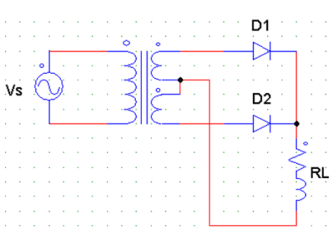
1. Rectifier circuit with resistive load using two Diode
The figure below is the schematic and waveform of a two half cycle rectifier circuit with load R=10 Ohm.
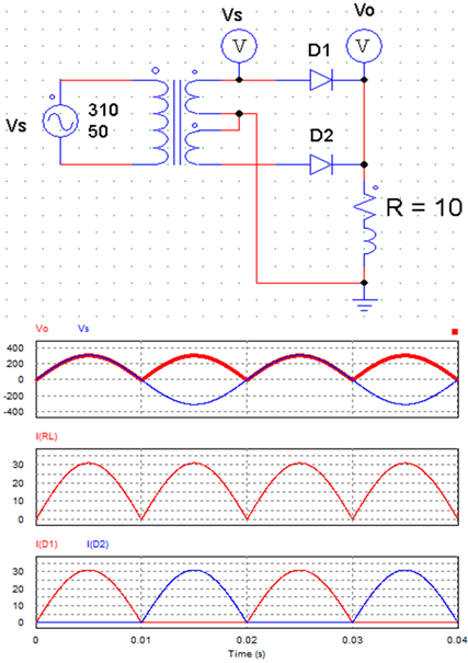
Two-half cycle rectifier circuit with resistive load
– Working principle:
+ As you can see: Looking at the waveforms of the 2 diodes, we see that Diode D1 conducts electricity in the positive cycle and diode D2 conducts in the negative cycle. Therefore, the AC voltage is rectified in both cycles. And the voltage and current waveforms in this case are the same as the full-wave bridge rectifier circuit.
+ In the positive cycle: Diode D1 is forward biased, so it conducts electricity, while D2 is reverse biased. The current is now through D1, through R, so the output voltage is equal to the voltage of the secondary coil Vo = Vs.
+ In the negative cycle: Diode D2 conducts while D1 stops conducting, current flows through D2, through the load. Therefore, the direction of the current through the load is still the same as in the positive cycle, but the output voltage is equal to and opposite to the source voltage Vo = -Vs > 0.
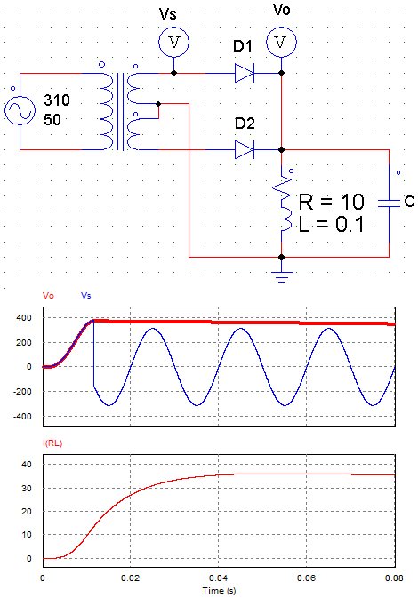
2. Rectifier circuit with RL load
The circuit diagram of a single phase 2 half cycle rectifier circuit with RL load is shown below, with L = 0.1H
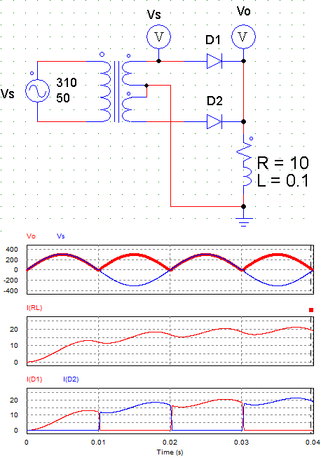
2 half cycle rectifier using 2 diodes with RL load
– The principle of the circuit:
+ Positive cycle: D1 conducts and D2 does not conduct, so the load voltage Vo = Vs.
+ In negative cycle: The source voltage is reversed, so D2 conducts and D1 turns OFF. Current through D2, through RL load, so the output voltage is still positive Vo = – Vs > 0.
The current on the load does not suddenly increase or decrease, so at the end of the half-cycle when the voltage reaches zero, the load current is still positive and will increase with each cycle until it reaches steady state.
3. The center tapped full wave rectifier with RLE load
In case we control a load with RLE component, we will simulate the operation of a circuit with a DC voltage component E in series with RL as follows:
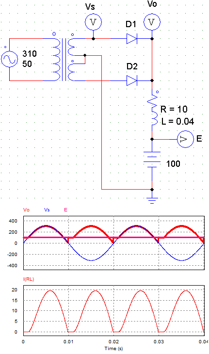
center tapped full wave rectifier circuit with RLE load
– Working principle:
+ If the source voltage is less than E then the diode is reverse biased so the output voltage is equal to E. But since the load is inductive, when the diode turns OFF then the load generates energy to generate current, which will continue maintain the conduction state of the diode
+ In the case of L = 0.04H, when the load runs out of energy but Vs < E, the output voltage Vo = E. The diode stops conducting, so the flow through the load is interrupted.
If we increase the value of L = 0.04H to L = 0.1H, when the load runs out of energy, Vs > E, so Vo = V. And D2 will conduct, so the current through the load is continuous.
4. Center tapped full wave rectifier circuit with filter capacitor
To smooth the output voltage, we will use a capacitor in parallel with the output load. The voltage of the load is the voltage across the two capacitor terminals.
center tapped full wave rectifier with filter capacitor
– Working principle:
+ In the first cycle, in the positive cycle when the source voltage increases, the capacitor begins to charge through diode D1. When the supply voltage reaches its maximum value and starts to decrease. then D1 stops conduction and the capacitor discharges through the load.
+ If the value of the capacitor is large enough, the voltage on the negative cycle will still be greater than the peak voltage value. Therefore diodes D1, D2 continue to be reverse biased so they do not conduct. Because the load is inductive, the current on the load increases slowly until it is established.
Therefore, we see that when using a capacitor in parallel with the load, the output voltage and current are flattened, and the output power is more stable.
5. Controlled rectifier circuit using two SCR
A controlled rectifier circuit will use 2 SCRs instead of diodes. The SCR is controlled by a synchronous signal with the source voltage, the excitation angle varies from 0 – 180 degrees.
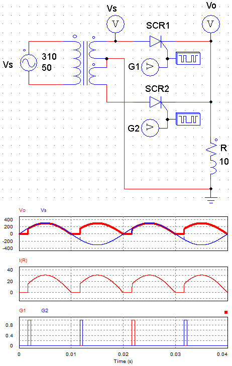
Full-wave Controlled Center-tap Rectifier with R load
– Working principle:
+ At the beginning of each cycle, when the Impulse at pin G has not appeared, the output voltage is 0V
+ In the positive cycle when there is an impulse at the G pin of SCR1, SCR1 immediately conducts. So the load voltage is equal to the source voltage: Vo = Vs.
+ In the negative cycle, when a pulse is applied to the G2 pin of SCR2, SCR2 will be turned on. The load voltage is opposite to the source voltage, so the current through the load is positive: Vo = -Vs >0, IR > 0
=> So compared to the uncontrolled rectifier circuit. The average voltage can vary from 0 to the average voltage of the circuit using the diode.
6. Controlled rectifier circuit with RL load using two SCR
The circuit diagram with RL load is similar to that in the R Load circuit. We just need to connect the resistor R with the inductor L. Depending on the L value, we have different output waveforms. The figure below is the waveform in 2 cases L = 0.1H and L = 0.008H
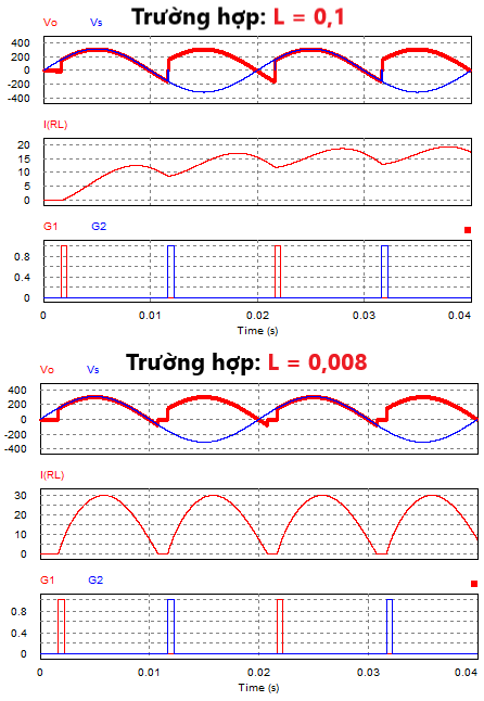
Waveform of controlled rectifier circuit with RL load
+ In the case of L = 0.1H, we see that the load current is always greater than 0 and increases gradually until it reaches the established value. Output voltage appears negative voltage, because when the source voltage changes polarity, the load generates energy to maintain SCR continues to conduct. Until a square pulse is applied to the G terminal of the other SCR.
+ In the case of L = 0.008H, we can see that the load current is interrupted. This is because the load runs out of energy before the next SCR conduction impulse.
7. Center tapped full wave rectifier with RLE load using 2 SCR
In this case: the load used has RLE components such as a DC motor. The output waveform is simulated in two cases as shown below.
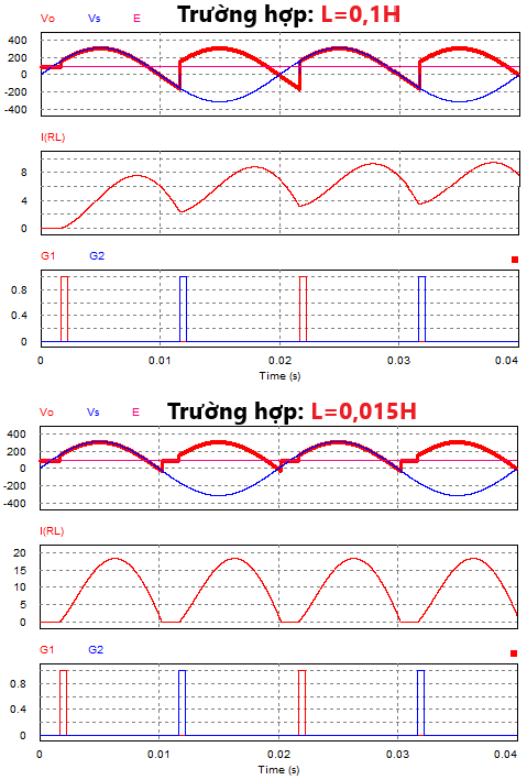
Center tapped full wave rectifier with RLE load using 2 SCR
+ In case the inductance value of the load is large enough (L = 0.1H). When the source voltage is reversed, the SCR is reverse biased. But the load acting as a generator continues to maintain the conduction state of that SCR. The load energy is large enough for the SCR to conduct until there is an impulse at the G pin of the next SCR. Since the output current is continuous, the output current input voltage waveform in this case is the same as the circuit using the RL load.
+ In the case of small inductance value (L = 0.015H). We see that when the voltage is reversed, the SCR can only lead a short distance. Since the load has now run out of energy and therefore the output voltage is now: Vo = E. Until the other SCR turns on, Vo = |Vs|.
Refer to the video on the principle of a two-half-cycle rectifier circuit using 2 diodes