In the previous article, we learned about the half-wave rectifier circuit. The disadvantage of half-wave rectifier circuit is low efficiency, large ripple because only allows voltage across the load at one half-cycle. Therefore, another type of rectifier circuit that is more commonly used is the full wave rectifier circuit.
In this post, we will learn about 6 full wave rectifier circuit diagrams, where the input voltage is rectified in both cycles. As a result, the average output voltage increases, and the ripple is lower.
1. What is a full wave rectifier circuit?
The full-wave rectifier circuit is a circuit that converts AC voltage into DC voltage, the input AC voltage is fully rectified in both cycles. The waveform of the output DC voltage has ripples with a frequency equal to twice the frequency of the mains voltage.
The output voltage waveform of the full-wave circuit
Indeed, if T is called the supply voltage period, the output waveform is repeated after a time of T/2. In other words, the frequency of the output waveform is twice the frequency of the input waveform. If compared with the half-cycle rectifier circuit in the previous post, this rectifier circuit has a larger average output voltage, smoother output waveform.
There are two types of full wave rectifier circuits. The first is using the center tapped transformer and the second method is using the bridge rectifier circuit. We will learn about the diagrams and principles of these circuits.
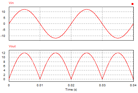
The formula for calculating the average output voltage and current:
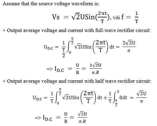
As we can see: Average DC output voltage across the load resistance is double that of a half-wave rectifier circuit
2. The center tapped rectifier
Firstly we will learn about the rectifier circuit using the center tapped transformer. Basically this circuit will include: transformer with center tapped, two diodes, resistive load.
For simplicity, in the simulation we will choose a transformer with a ratio of 1:2. This means, if we apply the input voltage Vin, then at the output of this secondary winding, we will get the 2 times Vin.
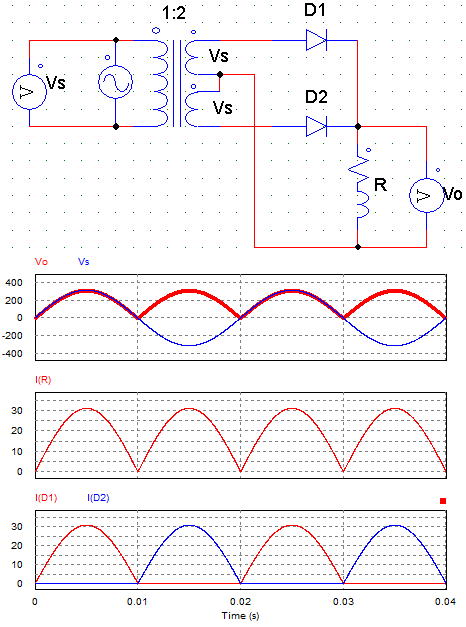
Center tapped full wave rectifier circuit diagram
– Working Principle:
+ During the positive cycle, only Diode D1 is forward biased, so diode D1 is conducting and this diode D2 remains off. Therefore the output voltage will be equal to the source voltage: Vo = Vs. Strictly speaking, Vo = Vs + VD1, but because the voltage drop across diode D1 is very small compared to the source voltage. So we assume that the diode is ideal.
Otherwise: Vs + Vo + VD2 = 0 => VD2 = -2Vs. Therefore, for this rectifier circuit, a parameter to pay attention to when designing the circuit is that the reverse voltage on the diode is twice the peak voltage. If we are applying an input signal which has a peak voltage of 10V then, the peak inverse voltage of the diode should be more than 20V.
So, while designing the circuit for the specific voltage we should always check the maximum reverse voltage which can be withstand by the diode
During the negative half-cycle, Diode D2 is forward-biased, allowing current to pass through it. During this time Diode D1 is reverse biased and will block current through it. The current through D2 and through the load is in the same direction as the positive cycle current. Therefore, we will have the current going through the load in the positive direction and the output voltage: Vo = -Vs > 0.3. Mạch chỉnh lưu cầu
Một loại mạch tiếp theo chúng ta sẽ tìm hiểu là mạch cầu chỉnh lưu toàn sóng. Ta sẽ xem xét một số mạch chỉnh lưu cầu cơ bản sau đây. Chi tiết bài viết về chỉnh lưu cầu xem lại bài viết bên dưới:
>>>See more: 11 bridge rectifier circuit diagram using diode, SCR with R, RL, RLE load
3. Full bridge rectifier circuit
3.1 Full wave rectifier bridge circuit diagram with using 4 diodes
The bridge rectifier circuit uses 4 diodes, the input voltage will be connected to the midpoint of each pair of diodes. The output is direct current, the positive pole is connected to the negative pole of the two Top diodes. The negative pole is the connector to the positive pole of the Bottom diodes
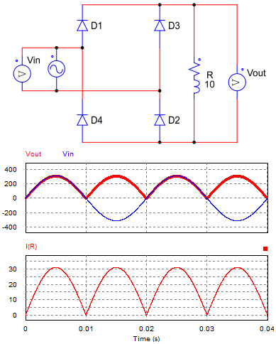
Bridge rectifier circuit diagram with load R using 4 diodes
Working principle of the circuit:
+ If we apply the sine wave as an input to this circuit, then during the positive half cycle this diode D1 and D2 will conduct. While this D3 and the D4 diode will remain OFF.
So, during the positive half cycle, the current will flow through D1, R, D2. Assuming this diode D2 and D4 are ideal. In that case, this input voltage will appear across this load resistor: Vo = Vs. So, the same input voltage will also appear at the output terminal.
+ Similarly, during the negative half cycle, these diodes D3 and D4 will remain OFF. And on the other end these diodes D1 and D2 will conduct.
So, during the negative half cycle, the current in the circuit will flow through D3, R, D4 and Vo = -Vs > 0 .So we are getting the output waveform for both half cycles. And during the negative half cycle also the current which is flowing through the load is in the same direction.
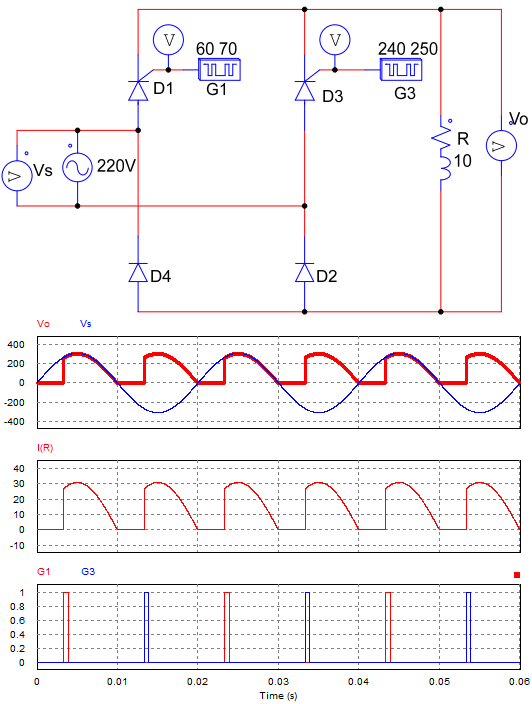
3.2 Full wave controlled bridge rectifier circuit diagram using 4 SCR
A controlled full-wave rectifier uses 4 SCRs instead of diodes. In this simulation circuit I will use a pulse generator that generates a signal in the form of a square pulse. The control signal is synchronous with the input voltage. The control angle in this case is 60 degrees.
Full wave controlled bridge rectifier circuit diagram
Working Principle:
+ In the positive cycle, when there is no control signal, all 4 SCRs will not conduct, so the output voltage is 0. When a control pulse is applied to pins G1, G2 of the two SCRs, immediately the two SCRs D1 and D2 is on, while D3 and D4 are still off. The voltage across the load is equal to the source voltage.
+ In the negative cycle, when there is no control pulse, all diodes do not conduct. When there is a control pulse then SCR D3, D4 conduct, SCR D1, D2 is now reverse biased. The current flows through the load in the positive direction and the output voltage has the same magnitude as the source voltage but opposite sign: Vo = -Vs > 0.
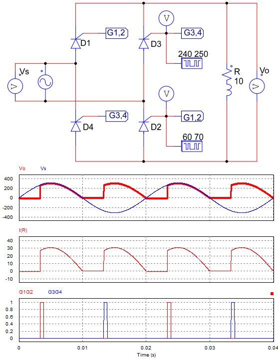
3.3 Symmetrical half controlled bridge rectifier
The asymmetric half controlled bridge rectifier uses two SCRs and two diodes connected to each column of the bridge circuit. The use of two diodes instead of two SCRs helps to reduce costs and widen the control angle (maximum excitation angle of 180 degrees).
The asymmetric half controlled bridge rectifier with R load
Explaination about the asymmetric half controlled bridge rectifier
+ During the positive cycle, when there is a control pulse G1, SCR D1 and Diode D2 conduct in series. Meanwhile, SCR D4 and D3 are reverse biased. So the current through SCR1, R, D2 and the output voltage is equal to the input voltage: Vo = Vs.
During the negative cycle, when the control pulse G2 is applied to the gate terminal of SCR D4, D3 and D4 conduct. But SCR D1 and diode D2 switch “OFF” as they are now reverse biased. The current through the load is the same direction as before and Vo = -Vs >0
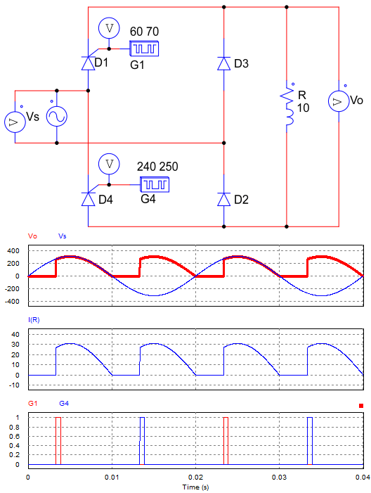
3.4 Symmetrical half controlled bridge rectifier circuit
The symmetrical semi-controlled bridge rectifier also uses two SCRs and two diodes, but the two SCRs are not wired to the same column. Circuit diagram as shown below:
Symmetrical half controlled rectifier bridge circuit
Working of half-control bridge rectifier:
The operation of this circuit is similar to that of the asymmetric bridge circuit. When there is a control pulse G3, SCR D1 and Diode D2 conduct, SCR D3 and Diode D4 remain off. When giving a control pulse G3 to the control pin of SCR D3 then D3 and D4 conduct, D1 and D2 turn OFF.
The waveform of the output voltage and the value of the voltage for the two cycles is similar to that of the asymmetric bridge circuit: Vo = |Vs|. The current flows through the load in one direction for the entire cycle.
4. Full wave rectifier circuit diagram with capacitor filter
We observe this output waveform, it is not completely DC voltage. Because still there is some periodic variation in this output waveform.
This periodic AC variation in the DC output voltage is known as the ripple. And this ripple can be reduced by using the filter circuit at the output of the rectifier.
Whether it is a center tapped rectifier circuit or a bridge rectifier circuit, the output voltage waveform is the same. Therefore, when we use the same type of filter capacitor, we will obtain the same DC voltage value.
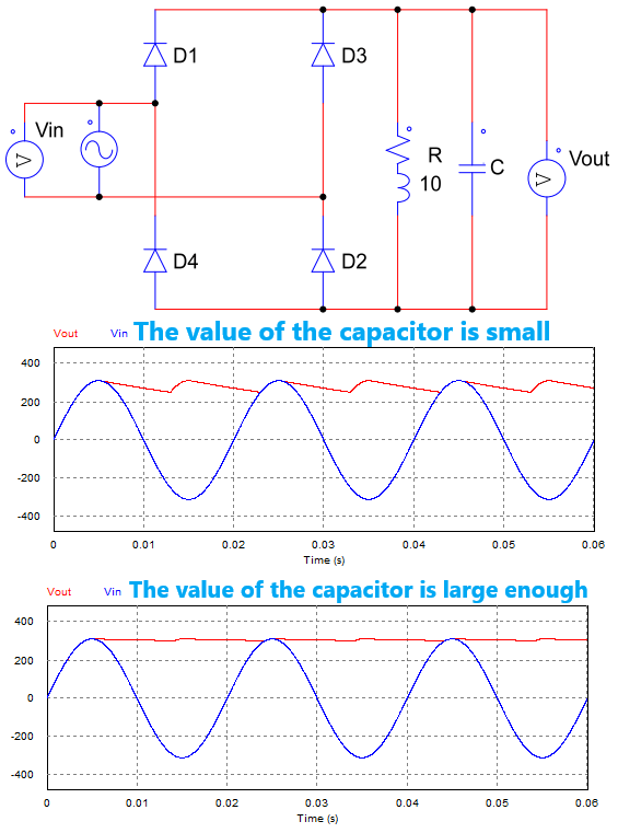
Full wave rectifier circuit diagram with capacitor filter
With this filter circuit, how well this ripple is removed, it depends on the value of this load resistance as well as this capacitor.
Working principle of rectifier circuit using filter capacitor
+ During the positive half cycle, this capacitor will charge up to the peak voltage. And once this capacitor gets fully charged, then this diode D1, D2 will become reverse bias. So, after the peak voltage, this capacitor gets discharged through this resistor R.
+ And whenever the voltage across the capacitor just goes below input voltage. Once again the capacitor starts charging. So, after that time once again this capacitor starts charging through Diode D3, D4.
When the voltage across the capacitor will become the peak voltage, then this diode D3, D4 will become OFF. And once again, now this capacitor starts discharging through this resistor R.
How to remove ripples
+ In the circuit, how well the ripple is removed, it depends on the RC time constant of this filter. For the better rejection of this ripple, the RC time constant should be much larger than this time period.
+ Suppose if this RC time constant is less than this time period T, in that case, this capacitor will get discharged rapidly. So, we will get more ripple in the output waveform. Avoid that, this RC time constant should be much larger than this T.
=> Since the resistive load is constant, we can increase the value of C to eliminate ripples
5. Comparison of full wave rectifier circuit and half wave rectifier circuit
– Advantages of full-wave rectifier circuit
+ Higher efficiency than half-wave rectifier circuit
+ During rectification, no voltage signal is wasted, so power loss is low.
+ The waveform of the output voltage is less rippled than that of the half-wave rectifier. Therefore, the average output DC voltage is higher.
– Disadvantage compared to half wave rectifier circuit
+ The disadvantage of full-wave circuits is that they are more expensive and tend to occupy more space and area. For a rectifier circuit with a centers tapped rectifier, the capacity of the circuit is limited by the capacity of the transformer.
Refer to the video explaining the principle of the full-wave circuit
>> Related posts:
Half wave rectifier circuit diagram (8 circuits)
Center tapped full wave rectifier (7 circuits)