In today’s article we will find out about a very popular type of component that is a MOSFET. What is Mosfet ? Their structure, principles, classification, application circuit diagram, we will learn in this article.
1. What is Mosfet?
MOSFET (Metal Oxide Semiconductor Field-Effect Transistor) is a type of transistor with fast switching and low switching losses. Unlike BJT transistors which are controlled by current, Mosfets are controlled by voltage.
MOSFETs require low gate power consumption, fast closing speed, and low switching losses. However, when the it conducts, its RON resistance is large. As a result, the power loss during conduction is large, which makes it impossible to develop into a large power device. Widely used in small power applications (several kW)
What is mosfet
2. Structure and operating principle
– Structure
MOSFETs come in two types: npn and pnp. The figure below shows the structure of an npn-type MOSFET. Between the Gate metal layer and the n+, p junctions there is a silicon oxide (SiO) layer. The basic advantage of MOSFETs is the ability to control the opening and closing by voltage pulses in the gate circuit.
Mosfet has 3 pins: Source (S), Drain (D) and Gate control pin (G). The G pin is completely isolated from the rest of the semiconductor structure by the SiO layer. Although this layer is thin, it has great electrical insulation
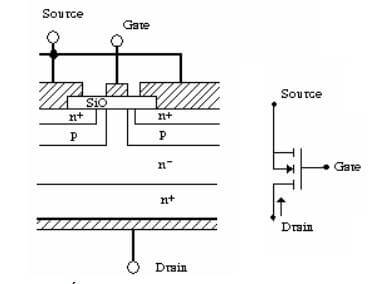
Structure and symbol of mosfet
– Working principle
When a positive voltage (VGS > 0) is applied between the G gate terminal and the S pin. The effect of the electric field through the SiO layer will pull electrons from the n+ layer into the p layer. A channel is formed between the Drain terminal and the Soucre terminal. Now if we put a voltage VDS between pins D and pin S, current will flow through this channel.
3. Characteristics of Mosfet
3.1 Characteristics
The V-A characteristic of an N-type MOSFET is shown in the figure below, which is similar to the V-A characteristic of BJT. The difference is that the control parameter is that the UGS voltage will replace the IBE current. (Mosfet is controlled by voltage, transistor is controlled by current)
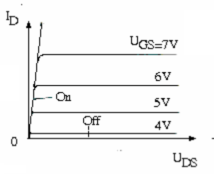
The V-A characteristic
Different from the SCR that we learned in the previous article. The voltage applied to the gate terminal must always be present for the MOSFET to conduct. Maximum control voltage UGS: ± 20V (depending on type). The most optimal voltage UGS to control the MOSFET can be from 12V – 15V.
The current entering the gate circuit is negligible, unless the circuit is in a transient state (switching on or off). Because at this time, the parasitic capacitor at the pole of the Mosfet gate charges or discharges, so this current is large. The charging and discharging time of the capacitor will affect the switching speed of the Mosfet.
Switching time is very small, from a few ns to hundreds of ns depending on the type of component. The internal resistance of the MOSFET (RON) as it conducts will depend on the voltage tolerance of the device. Therefore, MOSFETs usually have a low rated voltage corresponding to a small internal impedance and low loss.
However, the switching speed is fast, and the loss is low. Therefore, in applications with voltages from 300-400V, MOSFETs operate more efficiently than BJTs (at a frequency of several tens of thousands of Hz).
MOSFETs can be used up to a voltage of 1000V, a current of several tens of Amps. Or with a voltage of a few hundred Volts with an allowable current of about 100A.
3.2 Characteristic parameters
| Name | Maximum rated voltage | Rated average current | RON | Qg |
| IRFZ48 | 60V | 50A | 0.018Ω | 110nC |
| IRF510 | 100V | 5.6A | 0.54 Ω | 8.3nC |
| IRF540 | 100V | 28A | 0.077Ω | 72nC |
| APT10M25BNR | 100V | 75A | 0.025 Ω | 171nC |
| IRF740 | 400V | 10A | 0.55 Ω | 63nC |
| MTM15N40E | 400V | 15A | 0.3 Ω | 110nC |
| APT5025BN | 500V | 23A | 0.25 Ω | 83nC |
| APT1001RBNR | 1000V | 11A | 1.0 Ω | 150nC |
* Note: Qg is the amount of charge charged and discharged from the parasitic capacitance at the gate terminal when switching. Gate circuit loss power depends on Qg according to the formula: PG = Qg.UGS.fS; with fS is the switching frequency of the device.
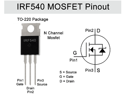
Refer to the datasheet of the N-channel Mosfet IRF540
4. Classification
There are two common types of MOSFET: N-channel MOSFET and P-channel MOSFET.
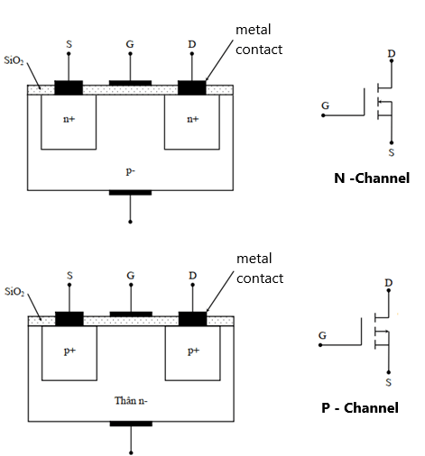
Classification
– N channel MOSFET: When the voltage applied to the gate terminal: UGS > 0, the current will go from D to S.
The N-channel MOSFET test circuit diagram is shown as shown below.
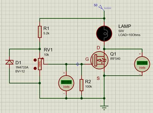
Operation principle of N – channel mosfet
The control circuit uses Zener Diode 12V to fix the voltage on the variable resistor RV1 to 12V, resistor R1 is used to limit the current for Zener. When the variable resistor RV1 changes from 0 to 10k, the control voltage (UGS) will change from 0 to 12V. And through simulation we can see that:
+ When the control voltage (UGS) > 4V, the MOSFET starts to conduct, but the voltage drop on the it (UDS) is large.
+ When the control voltage (UGS) > 10V, the UDS voltage does not change (UDS = 0.25V; Saturation Region).
Circuit simulation video:
– P channel MOSFET: When the control voltage applied to the Mosfet gate terminal is less than zero (UGS < 0), the current will go from S to D.
The P-channel MOSFET test circuit diagram is drawn as shown below.
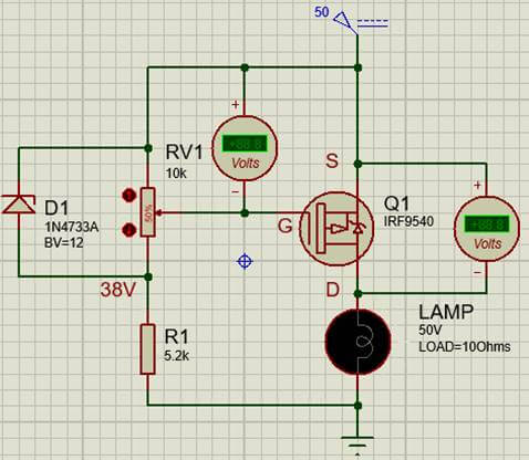
The principle of operation of the P- channel mosfet
Similar to the N-channel MOSFET driver circuit, using a 12V Zener diode to generate a 12V voltage source. When the variable resistor RV1 changes from 10K – 0 Ohm, the voltage USG = -UGS changes from 0 – 12V. Through simulation we can see:
+ When USG voltage > 4V, the P-channel MOSFET starts to conduct.
+ When USG voltage > 10V, the MOSFET is in saturation state (as a closed switch).
Circuit simulation video:
5. Application circuit
5.1 Control circuit using switch
Simple circuit that uses a switch to control the MOSFET. Thereby we can control turning on and off a lamp with high DC voltage. The power circuit uses high DC voltage (50V) and the control circuit uses low DC voltage (12V).
+ When the switch is in the open state: resistor R1 will pull the voltage at the gate terminal (UGS) to 0V, so the MOSFET does not conduct.
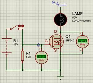
When the switch is open, the light is off
+ If the switch is in the closed state: the voltage at the gate terminal (UGS) = 12V, the MOSFET conducts like a closed switch, so the light is on.
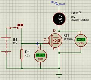
When the Switch is closed, the light is on
5.2 Control circuit with transistor
The circuit below controls the MOSFET with a buffer circuit using an additional npn transistor. Transistor acts as a switch like in the circuit above.
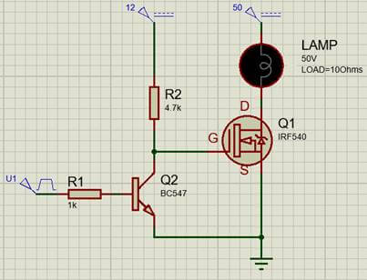
Control circuit using transistors
+ When the input voltage U1 is low, the transistor Q2 opens, the voltage UGS = 12V so Mosfet conduct makes the lamp turn on.
+ When the input voltage U1 is high, the transistor Q2 closes, the voltage UGS = 0V, the Mosfet does not conduct making the lamp turn off.
The advantage of this circuit is: The high level of the input signal can be from 3.3V or 5V, suitable for combining with microcontrollers.
Disadvantage: not suitable for application at too high frequency, because the parasitic capacitor inside the Mosfet will slow down the switching ability of the Mosfet. To solve this problem we will learn about the next application circuit.
5.3 Control circuit using totem-pole circuit
The circuit diagram below uses a buffer circuit consisting of 2 transistors NPN and PNP.
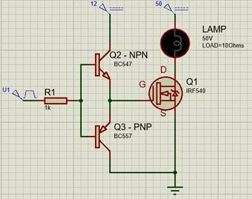
Control circuit using totem-pole circuit
+ When the input voltage U1 is high, Q2 conducts and Q3 does not conduct. At this time VGS = 12V so Mosfet conduct.
+ When the voltage signal U1 is low, Q2 does not conduct, the charge of the parasitic capacitor on the gate circuit is released, and at the same time Q3 conducts. Pull the UGS gate terminal voltage quickly to 0V, so the MOSFET doesn’t conduct.
The advantage of this circuit is that it can work with high frequencies, but the circuit is quite complicated.
When using a microcontroller to generate control pulses, an opto is often used to isolate the control circuit and the power circuit.
5.4 Control circuit with isolation
The circuit below uses the optocoupler PC817 to isolate the control circuit and the power circuit. The pulse generator circuit can use microcontrollers, or PWM circuits. In this circuit we will use IC555 circuit.
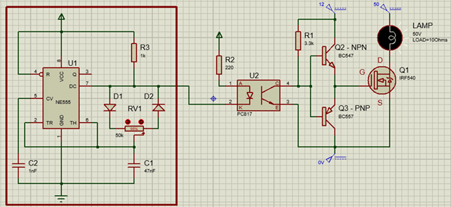
Circuit diagram of MOSFET driver with isolation
Working principle of electric circuit:
+ When the output voltage of the IC555 circuit is low, the Led of the PC817 will light up and make the transistor inside the optocoupler conduct. Then, Transistor Q3 conducts, voltage UGS = 0V, so the MOSFET does not conduct.
+ When the output voltage of the IC555 circuit is high, the LED optocoupler turns off, so the transistor inside the PC817 does not conduct. Voltage 12V through resistor R1 makes transistor Q2 conduct, as a result Mosfet also conducts.
Video simulating the principle of operation on Proteus software
This control circuit also has a disadvantage that it is impossible to reverse the DC motor. Therefore, for applications that need to be reversed, people use H-bridge circuits.
5.5 H-bridge using mosfet
The principle of motor speed control circuit by H-bridge circuit using MOSFET is to control each pair of MOSFETs alternately to change the direction of current flowing in the motor.
+ Assume that when Q1 and Q4 conduct, the motor rotates in the forward direction.
+ When Q2 and Q3 conduct, the motor rotates in the opposite direction.
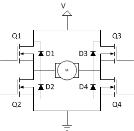
H-bridge circuit
**Note:
+ Two MOSFETs in the same column (Q1 and Q2, Q3 and Q4) must not be conducted at the same time to avoid causing a short circuit.
+ In order for the MOSFET to conduct completely, the voltage at the gate terminal of the Mosfet (UGS) must be from 12-18V. This leads to the control circuit of the H-bridge quite complicated.
>>> See more:
8 schematic diagrams of 3 phase rectifier circuit
4 star delta starter circuit diagram – Advantages and disadvantages