Output waveform and operating principle of single phase full wave controlled rectifier circuit with R, RL and RLE load
Circuit diagram and principle
1. Circuit diagram of full wave rectifier
The controlled rectifier circuit uses 4 SCR as shown in the figure. During each half-cycle, only two SCRs conducted at a time. SCR1 and SCR2 have the same control pulse signal, and SCR3 and SCR4 will have the same control signal.
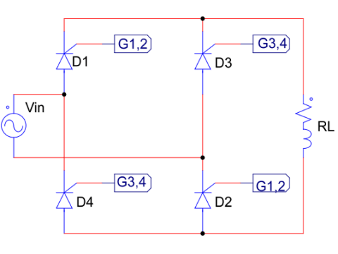
Circuit diagram of controlled rectifier
2. Working principle
+ Positive cycle: Vin > 0, SCR1 and SCR2 are forward-biased, so when there is a control pulse G1,2, they will conduct. Whereas SCR3 and SCR4 are reverse biased, they act as an open switch, not allowing current to pass through it.
+ Negative cycle: Vin < 0, SCR3 and SCR4 are forward-biased, so when there are G3, G4 pulses, they will conduct. SCR 3 and SCR4 act as a close switch. SCR1 and SCR2 are reverse biased and they act as a switch in the open state.
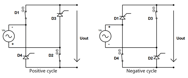
Working principle
Single phase full wave controlled rectifier circuit with R , RL , RLE load
1. Resistive Load
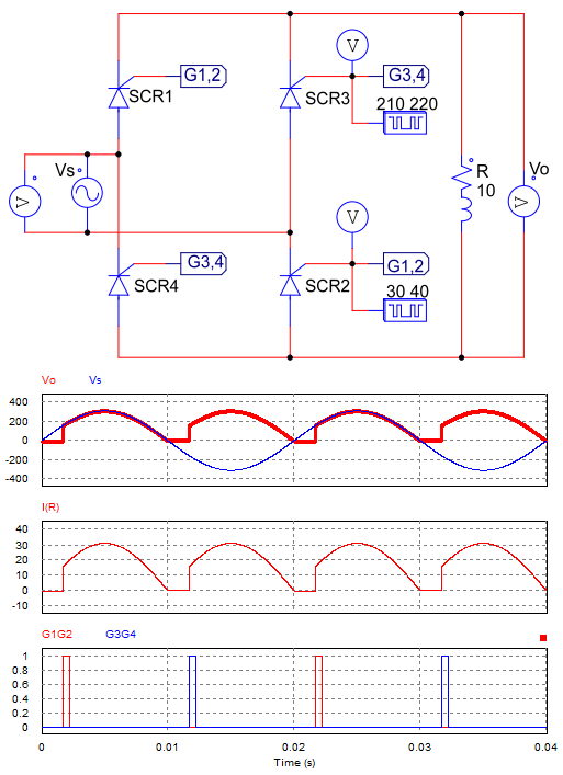
Single phase full wave controlled rectifier circuit with r load
We observe that, at the beginning of each half cycle, when there is no control pulse, the output current and voltage are zero. When there is a control pulse, the SCR conducts.
+ Positive cycle (SCR1 and SCR2 conduct): The output voltage is equal to the source voltage Vo = Vs
+ Negative cycle (SCR3 and SCR4 conduct): The polarity of the output voltage is opposite to the input voltage: Vo = -Vs.
2. RL Load
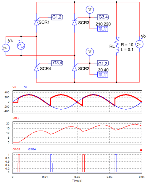
Single phase full wave controlled rectifier circuit with RL load
The two differences of a full-wave rectifier circuit with R load and RL load are:
+ The current with RL load does not increase or decrease suddenly. So the waveform between the output current and the output voltage is different. And the output current will tend to increase after each cycle. If the inductance of the load is large enough, the output current is continuous (figure above).
+ When the SCR changes from the conductive state to the off state, the load will generate energy to maintain that SCR continue to conduct. Therefore, after the polarity of the voltage is reversed and there is no control pulse, then the output voltage Vo < 0.
3. RLE load
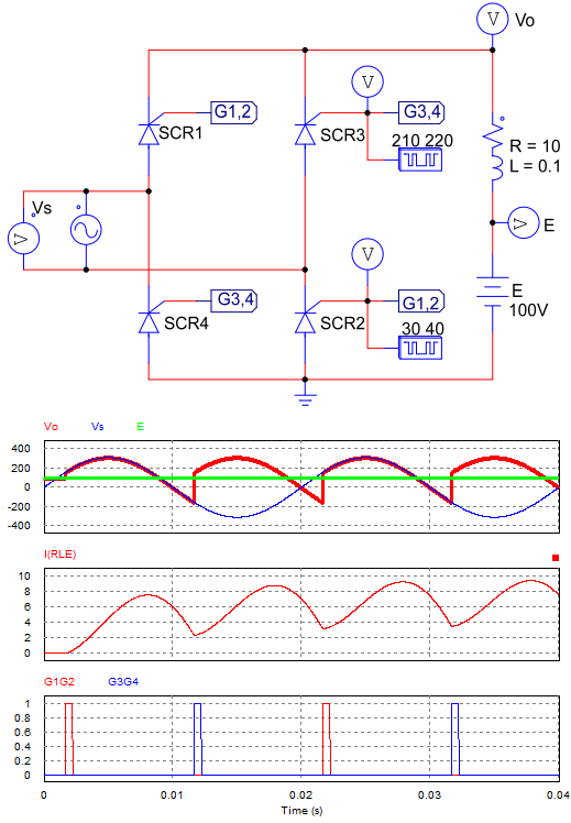
Single phase full wave controlled rectifier circuit with RLE load
When we use a load with components R, L, E, the output waveform of the circuit is drawn as shown in the figure above. If the SCR is conducting, the output waveform is the same as that of the RL load rectifier circuit. When no SCR is conducting (Io = 0) the output voltage is equal to E (Vo = E).
In case of RLE load with L = 0.1H, the load current is continuous. When we reduce the value of L = 0.02, the waveform of the circuit is as shown below.
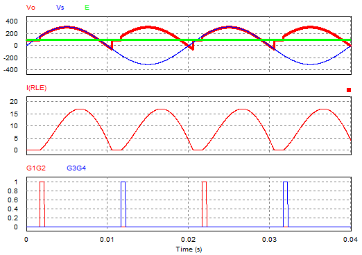
Output waveform with L = 0.02H
>>> Related posts:
Single phase full wave Rectifier (6 circuits)
Half wave rectifier circuit diagram (8 circuits)