In this post, I will explain the operation of the full-wave uncontrolled bridge rectifier circuit diagram (4 circuit diagrams). Some applications of bridge rectifier circuits.
1. What is full wave bridge rectifier circuit?
Full wave bridge rectifier circuit diagram is a circuit that uses to convert AC voltage into DC voltage using four diodes. The diodes are connected to form a closed bridge circuit. These rectifier circuits can also use transformers to vary the AC voltage level to suit each application.
What is bridge rectifier circuit?
The efficiency of a full-wave bridge rectifier is higher than that of a half-wave rectifier. The output voltage is present in both the positive and negative half-cycles of the AC voltage input. The average output voltage of this circuit is twice the average output voltage of the half-wave rectifier.
2. Full wave bridge rectifier circuit diagram (4 circuits)
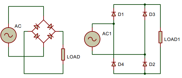
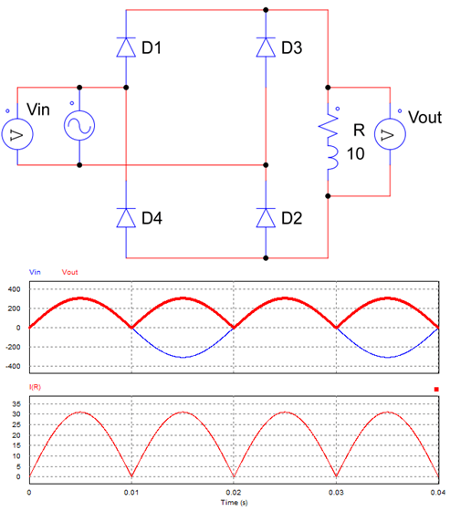
2.1 Rectifier circuit with resistive load
The circuit uses four diodes: D1, D2, D3, D4. The rectifier circuit diagram with R load is drawn as shown below:
Full wave bridge rectifier circuit diagram with R load
Operation Principle:
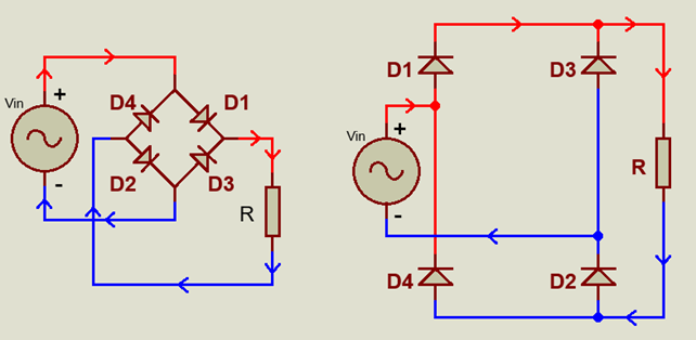
+ In the positive half cycle (Vs > 0): Diode D1 and D2 are forward biased while Diode D3 and D4 are reverse biased. So Diodes D1 and D2 will conduct, the current flows through D1, resistor, and D2 to return to the negative terminal of the source. If we consider Diode as ideal (when diode conducts voltage across it 0 VD = 0V) then: Vout = Vin.
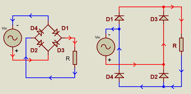
+ In the negative half cycle (Vs < 0): Diodes D1 and D2 are reverse biased, diodes D3 and D4 are forward biased. So diodes D3 and D4 conduct, they act as a close switch. Current from the power source through D3, resistor, and D4. We observe that in this case the current is in the same direction as the current in the positive half cycle: Vout = – Vs > 0, Iout > 0.
2.2 Full wave bridge rectifier circuit diagram with RL load
The output load is a resistor in series with an inductance L = 0.1H
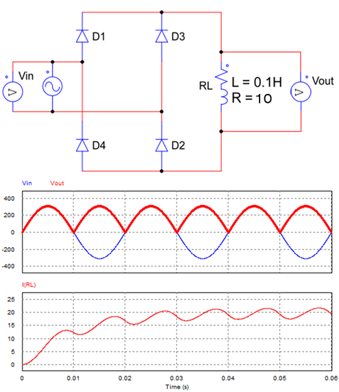
Full wave bridge rectifier circuit with RL load
Working principle:
The output voltage waveform of the rectifier circuit with RL load is the same as that of the rectifier circuit with R load. During the positive half-cycle, Diodes D1 and D2 will conduct. During the negative half-cycle, Diodes D3 and D4 will conduct.
However, we observe that the waveforms of the output voltage and the waveform of the output current are different. At the end of each half-cycle, when the voltage has reached 0V, the output current is still greater than 0. Therefore, the current will continue to increase after every half-cycle. When the output current is stable, the ripple of the output current is small.
2.3 Rectifier circuit with RLE load
For full-wave rectifier circuit with an RLE load, the output voltage will be: Vout = VRL + VE. We will simulate this circuit in two cases: L = 0.1H and L = 0.015H.
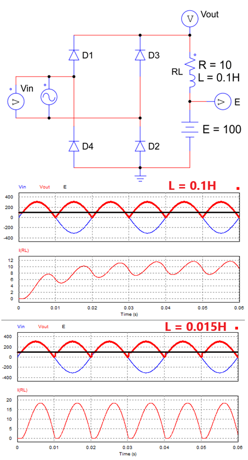
Rectifier circuit with RLE load
Working principle:
+ In the first positive half-cycle: The diodes are reverse biased because the supply voltage is less than E (Vs < E). The output voltage equals E: Vout = E, Iout = 0.
+ When the supply voltage is larger than E (Vs > E): the diodes D1 and D2 are forward biased, so they conduct. The output voltage will be equal to the voltage supply.
– RLE load With L = 0.1H:
+ Near the end of the positive half cycle: because the supply voltage is less than E, diodes D1 and D2 are reverse biased. The inductor is de-energized, so the load releases energy, creating a current in the same direction as the previous current. This current continues to make Diodes D1 and D2 conduct, until the end of the positive cycle.
+ In the first half of the negative cycle (|Vs| < E): Diodes D3 and D4 are reverse biased. But because the inductor emits current, diodes D3 and D4 continue to conduct. If the value of the inductor is large enough to maintain D3 and D4 until Vin > E, the output current is continuous.
– RLE load With L = 0.015H
When Vs < E, the diodes are reverse biased. Since the value of the inductor is small, it can only generate current for a short time. And then if the input voltage is less than E (Vs < E), the diode does not conduct: Io = 0 and Vout = E. So we observe that the output current is interrupted.
2.4 Application circuit
Full-wave bridge rectifier circuit diagram are commonly used in electrical equipment such as televisions, welding machines, ATX power supplies, phone chargers, computers, etc.
The figure below is a 5V DC power supply circuit diagram using a rectifier circuit. The Bridge rectifier circuit converts 12V AC voltage to DC voltage. Then we use IC 7805 to fix the output voltage to 5V.
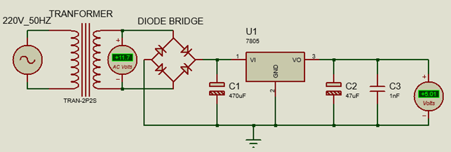
Power supply circuit using full wave bridge rectifier
The figure below is a voltage doubler that can use 110/220V AC to 310V DC. This circuit is used a lot in ATX power supplies. People will use high DC voltage to increase the capacity of the output source. The output voltage of this circuit is then changed by the pulse transformer to reduce it to 5V – 15V.
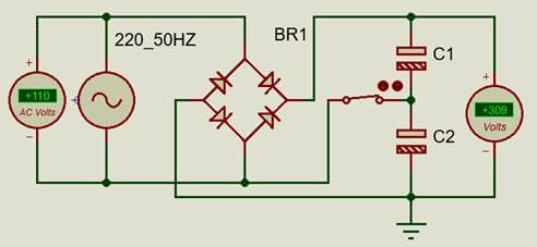
Bridge rectifier circuit in voltage doubler circuit
>>> See also: A basic introduction to a full wave bridge rectifier
>>> Related posts:
Star Delta Starter control circuit diagram schematic (4 circuits)